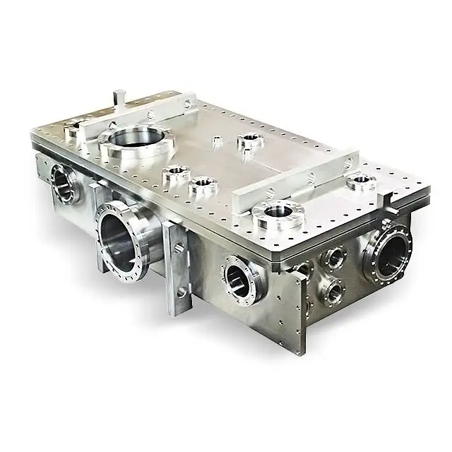
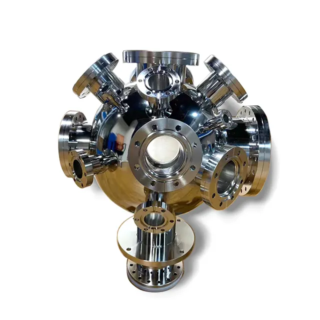
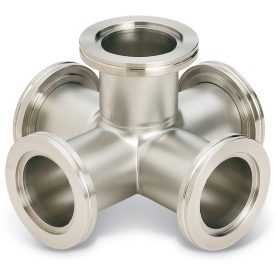
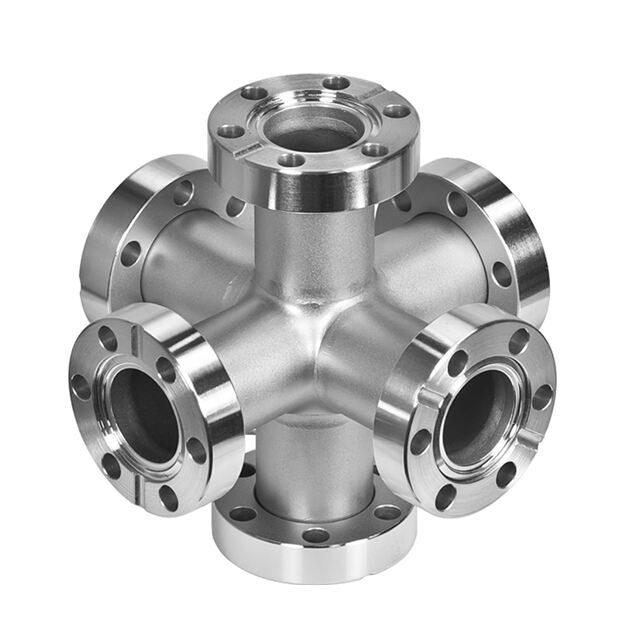
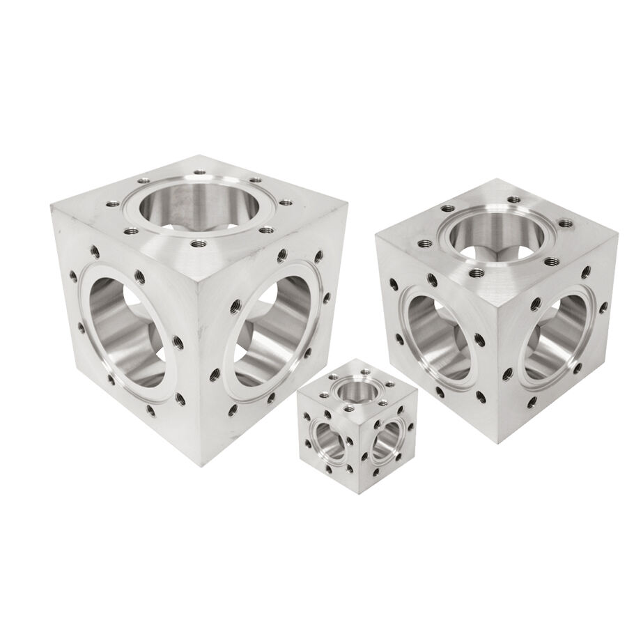
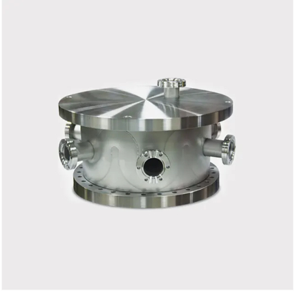
semiconductor vacuum chamber
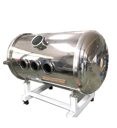
A semiconductor vacuum chamber is a sophisticated piece of equipment essential for modern semiconductor manufacturing processes. This highly engineered enclosure maintains an ultra-clean, controlled environment necessary for producing high-quality semiconductor components. The chamber operates by removing air and potential contaminants, creating a high-vacuum environment that typically reaches pressures between 10^-6 to 10^-9 torr. Inside this controlled space, various critical processes such as physical vapor deposition, chemical vapor deposition, and etching can be performed with exceptional precision. The chamber's design incorporates advanced materials and specialized sealing mechanisms to maintain vacuum integrity, while also featuring multiple ports for process gases, power delivery, and diagnostic equipment. Modern semiconductor vacuum chambers are equipped with sophisticated monitoring systems that continuously track pressure levels, gas composition, and temperature, ensuring optimal conditions for semiconductor processing. These chambers often integrate automated loading systems and robotic handlers to minimize contamination risks and increase production efficiency. The technology enables the creation of intricate microelectronic components with features measuring just nanometers in size, making it an indispensable tool in the production of advanced integrated circuits, microprocessors, and other semiconductor devices.